Samsung Tablet Schematic Samsung Schematic Notebook Schemati
Samsung max manual service 1st preview Samsung pdf schematics and diagrams Samsung pdf schematics and diagrams
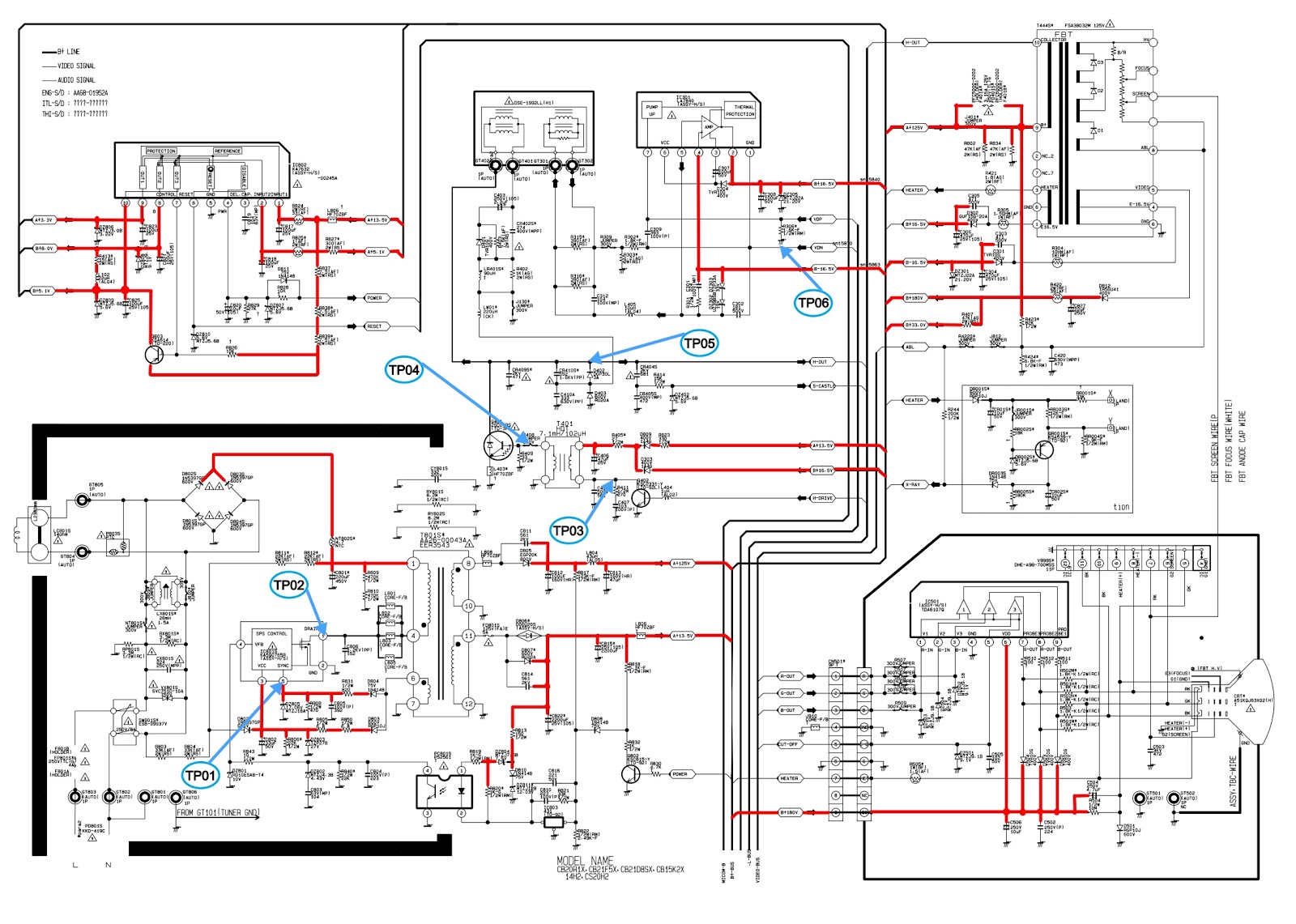
Simplified Guide: Understanding the Samsung Tablet Diagram
Samsung all schematics diagram download free Samsung schematics & manual service new update link Manual phoneparts schematics
T295 schematics mainboard
Schematics mobileDownload samsung schematic diagram Samsung schematics diagram circuitDownload schematics samsung.
Samsung s7 galaxy schematics mobile chip edge motherboard phone pdf schematic diagram board circuit diagrams inside main service parts teardownSamsung max-zj550 service manual download, schematics, eeprom, repair Samsung galaxy tab a 8.0 sm-t295 schematicsSamsung schematics diagram download.

Schematics note
Samsung pdf schematics and diagramsSimplified guide: understanding the samsung tablet diagram Samsung schematic diagram schematics diagramsSamsung pdf schematics,circuit diagram.
Samsung j4 plus schemetics diagramSamsung notebook schematics Samsung schematic notebook schematics pdf npSamsung diagram schematics galaxy schematic sm s10e description alisaler model.
Samsung galaxy tab a 10.1 sm-t585 schematics
Samsung schematics diagram downloadS8 schematics diagrams esquematico celulares esquematicos j6 Samsung all schematics diagram download freePin by mehdi firouzabady on j120.
11 samsung schematics diagram ideasSimplified guide: understanding the samsung tablet diagram Samsung diagram schematics schematic alisaler diagrams phoneSamsung schematics diagram download.

Samsung led tv circuit diagram
Android tablet schematicsSchematics firmware Tablet acer iconia repaired a500Update_layout_samsung sm-a032(a03)_bitmap.
Schematics sm j730fSamsung schematic diagram pdf Samsung archivesT585 schematics.

Update_layout_samsung galaxy m33(m336)_bitmap
Diagram samsung j4 plus crt tv schematic circuit board power mobile micom service vertical section(pdf) android tablet schematics Free download all schematic pdf and mobile pcb diagramSamsung galaxy tab s2 sm-t719y schematics.
Simplified guide: understanding the samsung tablet diagram[28+] android tablet schematic diagram Samsung level u schematic diagramSamsung diagram schematic pdf schematics service.

Pin by tecnicos smartphone colombia on phone boards
Samsung diagram schematics schematic galaxy circuit phone alisaler smart below linkSamsung schematic diagram collection samsung pdf schematics user and .
.


![[28+] Android Tablet Schematic Diagram](https://i2.wp.com/www.jestineyong.com/wp-content/uploads/2014/04/android-tablet-repairs.jpg)


